Key Benefits of Our Microscopy Products
We specialize in supplying a wide variety of high-purity materials for various scientific and technological applications. Some of the benefits of these products include:
Electron Microscopy (SEM, TEM): Materials like high-purity metals, ceramics, and advanced composites for sample preparation, supporting structures, and calibration standards
Confocal Microscopy: Specialized substrates and coatings optimized for specific fluorophores and improved image quality in fluorescence microscopy
Atomic Force Microscopy (AFM): Materials with well-defined surface structures and properties for calibration and characterization of AFM tips
Our products also provide improved image resolution: High-purity materials often exhibit minimal defects and impurities, leading to clearer and more accurate microscopy images


Supporting Research and Industry
In industries as varied as aerospace, automotive manufacturing, semiconductor manufacturing, food and beverages, and healthcare, microscopes have enabled unequaled leaps in the understanding of the properties of materials.
They enable advances in cancer research, stem cell research, cell biology, neuroscience, optogenetics, nanoelectronics, and more.
Additionally, the integration of advanced technologies such as deep learning, the internet of things, high-definition display modalities, and Extended Ultraviolet Lithography (EUVL) will continue to fuel demand.
We see our customers use our materials in various microscopy techniques, including optical, scanning electron, and transmission electron microscopy. They have been instrumental in investigating the morphology, texture, structure, and chemical composition of materials, enabling characterization and quality control.
Steering You Through Nanotechnology
Nanotechnology is a multidisciplinary field spanning sciences such as physics, biology, chemistry, materials science, and engineering that seeks to characterize structures and processes at molecular and atomic scales.
Since optical microscopes do not provide adequate resolutions at these scales, more powerful tools, such as electron and focused ion beam microscopes, are employed.
In regenerative medicine, for example, stem cells and other tissues are studied for the purposes of tissue engineering. High-resolution microscopes also enable advances in optogenetics, where the effects of light on individual neurons are studied.



Helping You Tackle the Growth of Semiconductors
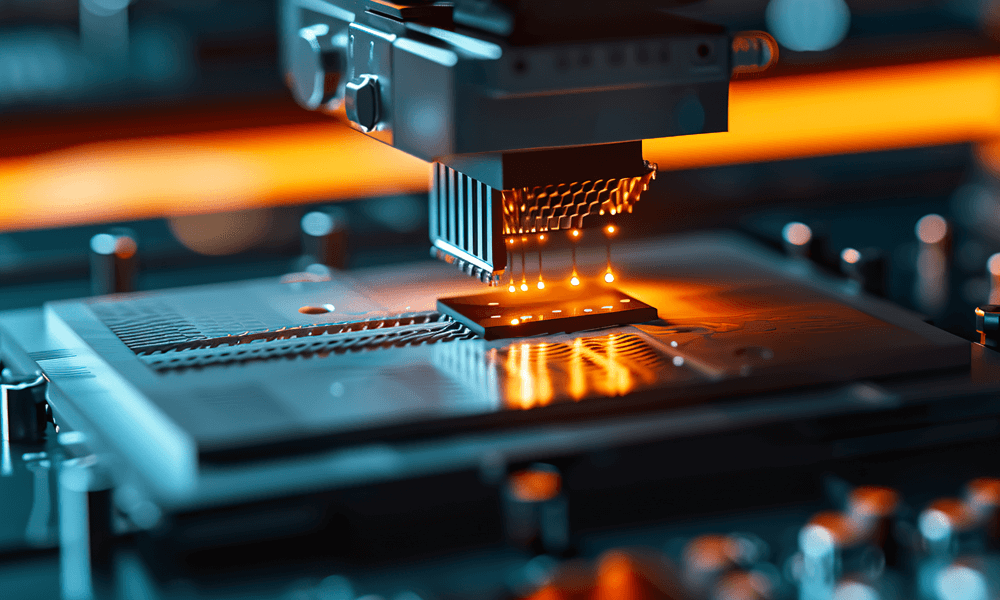
The exponential growth of the internet of things (IoT) has triggered a demand for integrated circuits, sensors, microcontrollers, memory chips, and other devices.
High-resolution microscopy enables atomic-level evaluation of gate structures, optoelectronic devices, packaged devices, nanotransistors, quantum dots, and more.
It is equally pivotal in pinpointing sources of failure to improve the manufacturing of these devices.
Empowering You with Our Materials Science Expertise
Materials scientists make extensive use of microscopy for the chemical and structural analysis of alloys, polymers, ceramics, biomaterials, and more.
The increasing sophistication of materials will continue to drive the demand for microscopy.
Goodfellow applies extensive materials expertise that meets the complex needs of microscopy.
Tungsten, for example, is a relatively inert metal resistant to acids, alkalis, and oxygen. With the highest melting point of all metals, it is relatively easy to work. However, being prone to impurities, tungsten can become extremely brittle and difficult to fabricate.


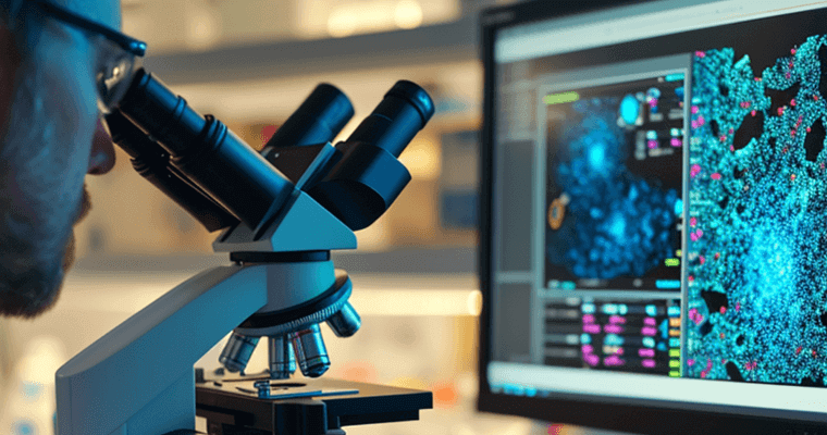

Driving Advances Through Academia and Research
Microscopes fulfill an increasingly critical function in research and development. They enable advances in cancer research, stem cell research, cell biology, neuroscience, optogenetics, nanoelectronics, and more.
Microscopy is an increasingly powerful tool that drives innovation while also being driven by innovation.


Using Silicon for a Breakthrough in Microscopy
Challenge:
A science team at Cornell University was limited by the capability of imaging tools, in their attempt to probe into the atomic structure of sulfur using a transmission electron microscope probe. The structure of molybdenum disulfide (MoS2), is an inorganic compound that shows great promise for building thin, flexible electronics. They were experiencing raised energy levels of the electron beam that resulted in sulfur atoms becoming displaced.
Solution:
After sourcing materials from Goodfellow, they were able to create an electron microscope pixel-array detector (EMPAD), built on a slab of silicon half a millimeter thick. This was able to capture all the energy from the electrons in the beam and the detector could separate the tiny fraction of deflected electrons from undiverted electrons in the beam.
Materials Challenges in Optical Microscopy
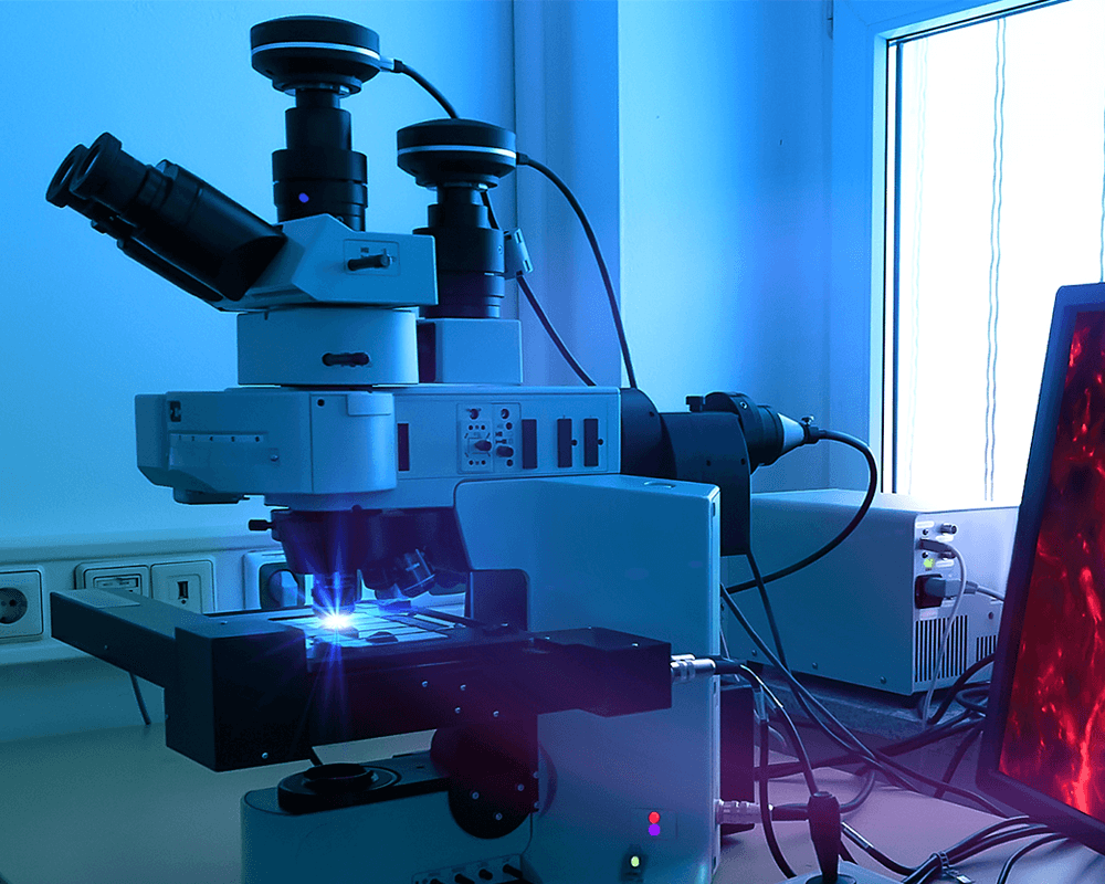
An optical microscope comprises an optical system, including an eyepiece, objective and other lenses, and hardware components holding the optical system in place and enabling adjustments to be made such that:
- Lenses are fabricated from optical glass, mainly made from silicon dioxide but also contain other elements such as boron oxide, zinc oxide, or lead oxide. Lenses may also be coated with an anti-reflective coating, typically magnesium fluoride.
- Encasing hardware is fabricated from steel (or steel and zinc alloys) using precision metalworking equipment. Sometimes an inexpensive, hard plastic such as acrylonitrile-butadiene-styrene may be used instead.
- If a mirror is included, it is typically fabricated from a strong glass such as Pyrex® (containing aluminum oxide, silicon dioxide, and boron dioxide). In the event a light bulb is also included, it is fabricated from glass, which encapsulates a tungsten filament and wires made of iron and nickel.
- If a camera is also included, it incorporates lenses fabricated from optical glass, as well as a metal or plastic casing.


Materials Challenges in Electron Microscopy
Electron beams form the operational core of electron microscopes. In these microscopes, thermionic sources generate electrons as heat is applied. Similar to how ordinary incandescent bulbs generate light, a metal filament or crystal is heated until electrons at the surface have enough energy to escape and form a beam. Thermionic sources may be created from:
- Tungsten filaments, which can be relatively cheap and easy to maintain. However, just as in ordinary lightbulbs, these filaments gradually lose mass due to evaporation, eventually resulting in breakage. As a result, tungsten filaments have the shortest lifetime of any thermionic source. Also, because of their high operating temperature, they generate a broader beam spread together with lower brightness, resulting in reduced image quality.
- Cerium hexaboride (CeB6) and lanthanum hexaboride (LaB6) sources comprise a single crystal of each molecule, respectively. They operate at lower temperatures than tungsten, reducing their beam spread and increasing their brightness. They also have a significantly longer lifetime than tungsten. The disadvantage, however, is they also need to be operated at higher levels of vacuum, resulting in a higher overall cost.
- Besides thermionic sources, field emission sources (or field emission guns) apply a strong electrostatic field to the tip of a tungsten wire to induce electron emission through quantum tunneling.
What's New


